“GPU computing has achieved great success in semiconductor design, simulation, and manufacturing. But as process technology shrinks, the physics is becoming increasingly difficult to simulate. At the same time, the sensor data is growing exponentially. This creates an opportunity for data-driven approaches like deep learning to complement physical models. We look forward to supporting CDLe and their efforts to achieve breakthrough results.”
The Center for Deep Learning in Electronics Manufacturing (CDLe) was a five-year (2018-2023) alliance of industry leaders who recognized deep learning’s problem-solving potential for electronics manufacturing. These companies came together to pool talent and resources to advance the state-of-the-art in deep learning for the unique electronic manufacturing problem space and to accelerate the adoption of deep learning in each company’s products to improve our respective offerings for our customers.
Proven Path to Deep Learning Success
Electronics manufacturing companies doing Deep Learning (DL) have found that it’s easy to get to a DL prototype, but it’s harder to get from “good prototype” results to “production-quality” results.
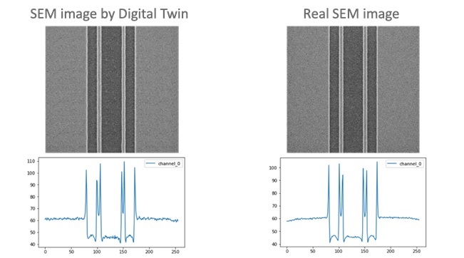
DL for electronics manufacturing is inherently more difficult because the level of accuracy required is orders of magnitude higher than typical DL applications. Reaching this high level of accuracy requires masses of training data, including serious anomalous conditions that (thankfully) rarely occur in production.
This lack of data – particularly anomalous data – creates a data gap between prototype- and production-quality DL applications. CDLe has successfully completed over 30 production DL projects for electronic manufacturing by using digital twin technology to bridge this data gap.
Digital Twins Bridge the Data Gap
Digital twins – virtual representations of actual processes, systems, and devices – are a key tool for creating the right amount of the right kind of data to train DL networks successfully. For many error conditions, digital twins are the only way to create enough anomalous data to properly train the networks to recognize these conditions.
For more details on the use of SEM digital twins, watch this video by Ajay Barawal, director of CDLe, or read an article covering this topic for Semiconductor Digest.
Videos
SPIE Photomask Technology 2021: A General Formula for Deep Learning Success in Semiconductor Manufacturing
A Deep Learning Mask Analysis Toolset Using Mask SEM Digital Twins
Thomas Kurian of Mycronic describes work at CDLe to identify “Mura” on flat panel display (FPD) masks

Ajay Baranwal, Director of CDLe, describes five deep learning recipes for the semiconductor mask making industry
CDLe Celebrates One-year Anniversary
About Deep Learning in Electronics Manufacturing
Meet Ajay Baranwal, the new CDLe Director
Aki Fujimura and Steve Teig talk about Deep Learning
Publications
Semiconductor Engineering: Center For Deep Learning In Electronics Manufacturing: Bringing Deep Learning To Production For Photomask Manufacturing
news • November 16, 2023
Using digital twins to bridge the data gap that keeps deep learning prototypes from moving to production.
SPIE Webinar: "Going Deep: Without the Right Data, Deep Learning Stops as a Prototype"
news • August 30, 2022
Presented by Aki Fujimura, D2S, Inc.
SPIE Photomask Technology 2021: A SEM-based DL diagnosis system for identifying VSB mask writer defects
news • September 30, 2021
Presented by Ajay Baranwal, Center Director of CDLe at the SPIE Photomask Technology Conference, September 29, 2021
SPIE Photomask Technology 2021: A general formula for deep learning success in semiconductor manufacturing
news • September 30, 2021
Presented by D2S CEO Aki Fujimura at the SPIE Photomask Technology Conference, Sept. 29, 2021
Semiconductor Digest: Automating Mask SEM Analysis Using Digital Twins
news • May 26, 2021
Article from Ajay Baranwal of the CDLe, Noriaki Nakayamada of NuFlare, Mikael Wahlsten of Micronic, and Aki Fujimura of D2S
A Deep Learning Mask Analysis Toolset Using SEM Digital Twins
publication • October 16, 2020
Ajay Baranwal, Director of CDLe, Presented at 2020 Photomask Technology Conference
EE Times: Digital Twins: Bridging the Data Gap for Deep Learning Success
news • June 1, 2020
Aki Fujimura explains the critical role of digital twins in deep learning
Semiconductor Engineering: How And Where ML Is Being Used In IC Manufacturing
news • April 1, 2020
Experts at the Table, Part 2: ML is playing a bigger role in metrology and lithography, but it can’t replace physics-based models.
Semiconductor Engineering: What Machine Learning Can Do In Fabs
news • March 25, 2020
Experts at the Table: It’s not as accurate as simulation, but it’s a lot faster.
The Mycronic Path Back to Semiconductors and into Deep Learning
publication • February 25, 2020
Presented at SPIE eBeam Initiative lunch by Thomas Kurian from Mycronic
Bridging the gaps: Deep learning to the manufacturing electronics factory line
publication • November 14, 2019
Presented at SEMICON Europa 2019 by Javier Cabello from Mycronic
Five Deep Learning Recipes for the Mask Making Industry
publication • September 23, 2019
Ajay Baranwal, Director of CDLe, Presented at 2019 Photomask Technology Conference
SPIE 2019: GPU Accelerated Simulation Enables Deep Learning
publication • February 26, 2019
Leo Pang of D2S explains why GPU-accelerated simulation is so important to deep learning
Going deeper with AI – how Mycronic’s new collaborative deep learning center can help unlock the value of AI
publication • January 31, 2019
Mikael Wahlsten, Director and Product Area Manager for Photomask Generators at Mycronic, gives his insights into the idea behind the new collaboration and what it can mean for Mycronic customers in the near future.
Semiconductor Engineering: Machine Learning For IC Production
publication • January 18, 2019
Experts at the Table, part 3: Where can this technology be applied and what’s ahead.
Semiconductor Engineering: Machine Learning Moves Into Fab And Mask Shop
publication • November 14, 2018
Experts at the Table, part 2: Where can this technology be applied, why it is taking so long, and what challenges lie ahead.
Semiconductor Engineering: Will machine learning and AI improve chip manufacturing?
publication • October 18, 2018
NVIDIA, NuFlare, Mycronic and D2S executives give their perspective
Deep Learning is Going to Improve Mask Manufacturing Too
publication • September 30, 2018
Aki Fujimura pens an editorial on Deep Learning for the BACUS Newsletter
Deep Learning Primer: Data is the New Source Code
publication • September 19, 2018
Presentation at 2018 Photomask Technology Conference
Semiconductor Engineering: Week in Review - Deep Learning Center
news • September 14, 2018
NuFlare, Mycronic, and D2S Partnership tops the manufacturing news for the week
Center for Deep Learning in Electronics Manufacturing Announced by Industry Leaders
press-release • September 12, 2018
Alliance of NuFlare Technology, Mycronic and D2S using NVIDIA Technology